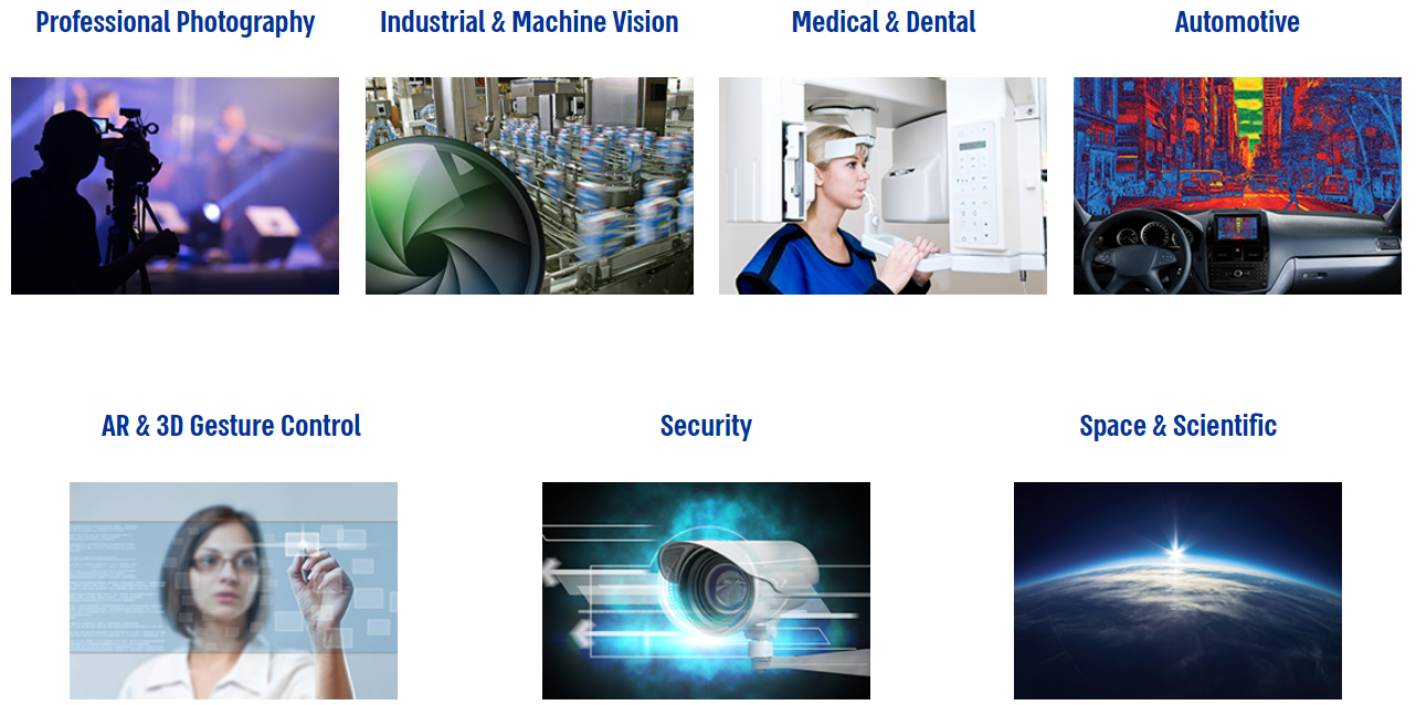
Tower Semiconductor’s worldwide recognized leadership in CMOS image sensors and pixel technology is derived from its vast experience and proven ability to supply sensors with best-in-class performance, customized to product and application needs. We provide our customers with high end, state of the art imaging solutions as well as unique customization processes enabling unmatched pixel design flexibility. The company’s extensive expertise in the imaging field combined with in-house CIS technology development enables Tower Semiconductor to meet the market’s rigorous requirements for leading-edge performance, advanced features and reduced die size.
Tower Semiconductor’s long-term investment in R&D and technical support keeps it at the cutting edge of CIS technology. By choosing Tower Semiconductor’s mature process, customers benefit from skilled experts who work to customize designs and provide rich solutions to meet their requirements and project needs.
Tower Semiconductor’s CIS technology is offered on three different platforms:
- 8” wafers, 180nm with aluminum backend (1)
- 8” wafers, 110nm with copper backend
- 12” wafers, 65nm with copper backend (1), (2)
(1) Stitching technology is currently available on 180nm and 65nm platforms (both two-mask and one-mask stitching) and soon will be also available on 110nm platform.
(2) On 65nm platform, our unique dual light pipe for high QE and high shutter efficiency (for global shutter pixels) is available
Power Management Markets Served
